
New Delhi, Aug 31: The government on Monday notified the Rs 1.27-lakh-crore Semicon 2.0 programme, spelling out eligibility and incentives across the semiconductor value chain, including 40 per cent fiscal support for silicon wafer fabs with a minimum investment of Rs 20,000 crore, and sweeteners for chip design.
India’s bold pitch to woo global investors and foster startups working on cutting-edge chip design comes at a time when semiconductors have emerged as a critical strategic resource globally, with the AI boom driving unprecedented demand for advanced chips and memory.
At the same time, growing concerns over supply-chain vulnerabilities and shifting geopolitics have pushed global players to expand semiconductor capacities and reduce dependence on concentrated production hubs.
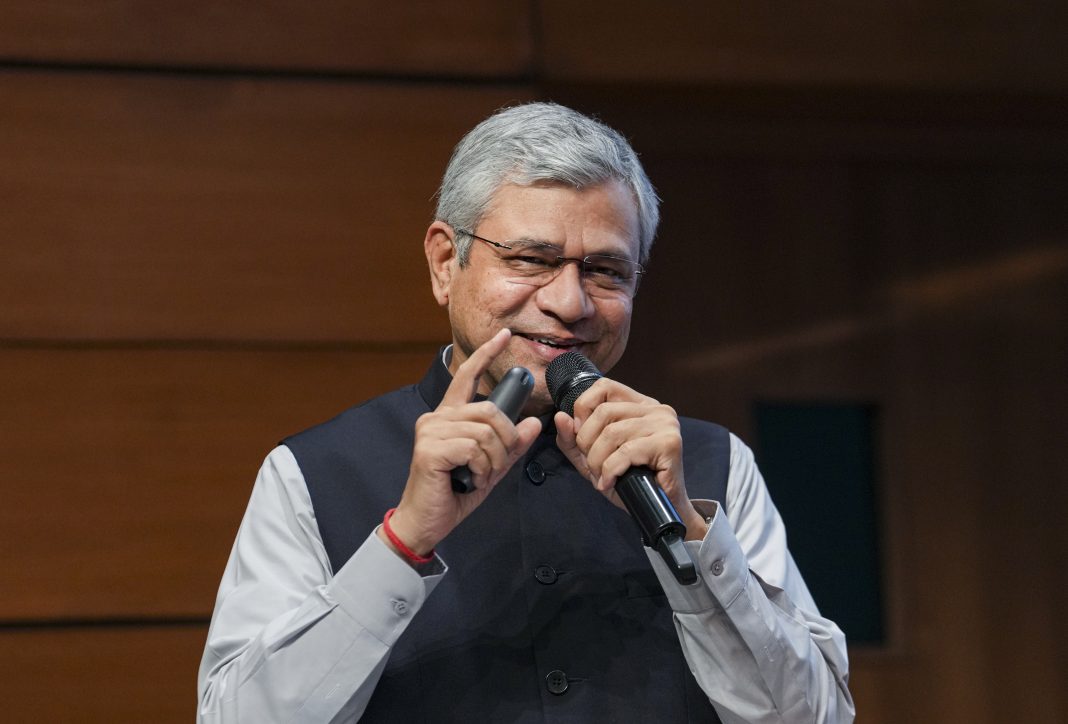
“In the coming years, close to 10 per cent of the global semiconductor industry’s market is expected to be in India,” IT Minister Ashwini Vaishnaw told reporters.
While the Semicon 2.0 scheme was approved by the Union Cabinet on July 15, 2026, Monday’s notification spells out the exact contours of the new programme, detailing how the Rs 1,27,500-crore outlay will be implemented, how incentives will be structured, and the eligibility thresholds for various categories.
Design forms the first of the scheme’s six pillars, with the government laying out a multi-pronged support framework spanning chips for strategic and critical infrastructure, commercial chip design, and incentives for deployment of indigenously-designed chips and IPs – all geared to build a self-reliant and competitive chip design ecosystem in India.
Within design, the first category targets strategic priorities, covering IPs, chips, System-on-Chip (SoC) and modules for critical and national infrastructure. Eligible companies must be incorporated and headquartered in India, have a significant domestic operational and manpower presence, and be Indian-owned and controlled.
They can participate independently or through consortiums, with fiscal and infrastructure support determined through competitive bidding under CDAC-issued request for proposals. The identification of the chips will be done by a high-level expert committee chaired by the Principal Scientific Adviser (PSA) and the National Security Adviser (NSA).
IP rights will be jointly owned by the applicant and C-DAC, and fiscal support will be disbursed based on RFP terms and conditions.
For commercial chip design, Semicon 2.0 supports India-headquartered companies owned or controlled by Indian citizens or OCIs, with IP and design files required to remain in India. Incentives include access to EDA tools, wafer fabrication, IP cores and validation infrastructure for design infrastructure support.
For product design-linked incentive, startups and MSMEs can receive seed funding of up to Rs 15 crore, or 50 per cent of project cost, and equity co-investment (beyond Rs 15 crore), while other eligible companies can access royalty financing or equity co-investment.
Separately, under the deployment-linked incentive, new IPs, chips and SoCs with no prior sales can receive a 9 per cent reimbursement on net sales for five years, capped at Rs 30 crore per application and Rs 120 crore per company.
The scheme, notified by the Ministry of Electronics and Information Technology (MeitY), covers six pillars and 10 categories in all, spanning chip design, semiconductor equipment and materials, fabrication, packaging, research and development, and talent creation.
For silicon semiconductor wafer fabs, the government has prescribed a minimum investment of Rs 20,000 crore and minimum revenue of Rs 7,500 crore in any of the three financial years preceding the application. Eligible fabs must have a capacity of at least 40,000 wafer starts per month on 300-mm wafers and own or possess production-grade licensed technology.
Projects under this category will be eligible for fiscal support equivalent to 40 per cent of eligible capital expenditure on a ‘pari-passu’ basis – though the incentives are lower than last time around.
The central fiscal support for such fabs has been scaled down to 40 per cent from 50 per cent under the previous scheme, with the government attributing this to states now offering additional incentives equivalent to about half of the Centre’s support, thus taking the effective government assistance to around 60 per cent.
IT Secretary S Krishnan said that the risk perception too has changed since the first scheme. With semiconductor projects now taking shape in India, the earlier uncertainty over whether such facilities could be established in the country has diminished, strengthening investor confidence.
Compound semiconductor, photonics, sensor and discrete semiconductor fabs will get 35 per cent support. Here, the minimum capital investment has been pegged at Rs 500 crore and revenue threshold at Rs 200 crore.
For display fabs, the scheme offers 35 per cent support, with investment thresholds varying by technology. OLED and LCD fabs require a minimum investment of Rs 10,000 crore and revenue of Rs 5,000 crore, while Micro LED projects need investment of at least Rs 1,500 crore and revenue of Rs 600 crore.
Incentives are on offer for machines and materials too – Semicon 2.0 offers 30 per cent capex support across equipment, semiconductor-grade raw materials and testing facilities, with equipment manufacturing also eligible for 2-10 per cent production-linked incentive.
Advanced semiconductor R&D and talent-development projects can receive support of up to 75 per cent of project cost, including state incentives.
For ATMP/OSAT facilities, Semicon 2.0 differentiates between advanced and legacy packaging. Advanced packaging, including 2.5D/3D packaging, wafer-level chip-scale packaging, heterogeneous integration and advanced substrates, will receive fiscal support of 35 per cent of eligible capex, while legacy packaging will get 25 per cent.
Both require a minimum investment of Rs 1,000 crore and revenue of Rs 200 crore in any of the three preceding financial years, with applicants required to own or possess production-grade licensed technology. (PTI)